PHYSICO-CHEMICAL PROCESSES IN VERTICAL-DOUBLE-DIFFUSED METAL-OXIDE-SEMICONDUCTOR FIELD EFFECT TRANSISTORS INDUCED BY GAMMA-RAY IRRADIATION AND POST-IRRADIATION ANNEALING
Abstract
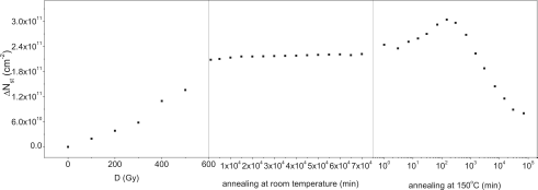
The behavior of commercial power Vertical-Double-Diffused Metal Oxide Semiconductor Field Effect Transistors (VDMOSFETs) during gamma-ray irradiation and subsequent annealing at room and elevated temperature was investigated. The densities of radiation-induced fixed traps and switching traps were determined from the sub-threshold I-V curves using the midgap technique. It was shown that the creation of fixed traps dominated during irradiation. The experimental results have also proved the existence of latent switching traps buildup process during annealing at an elevated temperature. This increase correlated with the decrease in fixed trap density. Physical and chemical processes responsible for the threshold voltage shift during irradiation have been analyzed on the basis of interactions between secondary electrons released by gamma photons with covalent bonds and . H-W model has been used for the explanation of processes leading to latent switching traps buildup at an elevated temperature and its passivation at late annealing times.
FIZIČKO-HEMIJSKI PROCESI U VDMOSFET-u IZAZVANI GAMA-ZRAČENJEM I OPORAVKOM POSLE ZRAČENJA
Istraživano je ponašanje snažnih VDMOSFET-a za vreme ozračivanja gama zračenjem i kasnijeg oporavka na sobnoj i povišenoj temperaturi. Gustine defekata u oksidu i na međupovršini su određivane iz predpragovske karakteristike korišćenjem midgap metode. Eksperimentalni rezultati su potvrdili postojanje latentnog porasta površinskih stanja na Si-SiO2 međupovršini koji se stvaraju za vreme oporavka na povišenoj temperaturi. Njihov porast je praćen smanjenjem zahvaćenog naelektrisanja u oksidu. Fizičko-hemijski procesi koji dovode do promene napona praga za vreme zračenja su analizirani na osnovu interakcija između sekundarnih elektrona, oslobođenih gama fotonima i kovalentnih Sio – O i Sio – Sio veza. H-W model je korišćen za objašnjenje procesa koji dovode do pojave latentnog porasta površinskih stanja na Si-SiO2 međupovršini na povišenoj temperaturi kao i njihove pasivizacije tokom kasnijeg oporavka.
HIGHLIGHTS
- Herein, the commercial power Vertical-Double-Diffused Metal Oxide Semiconductor Field Effect Transistors (VDMOSFETs) was studied
- VDMOSFETs behavior during gamma-ray irradiation and subsequent annealing at room and elevated temperatures was investigated
- The creation of fixed traps dominated subject to irradiation
- Latent switching traps buildup process existed during the annealing at elevated temperatures
- H-W model explains processes leading to latent switching traps buildup at elevated temperatures and its passivation at late annealing times
Full Text:
PDFRefbacks
- There are currently no refbacks.
ISSN 0354-4656 (print)
ISSN 2406-0879 (online)